find your perfect postgrad program
Search our Database of 30,000 Courses
Engineering Research: Ground-breaking graphene
A single material can probe the secrets of antimatter and may soon be a key component of everyday items, such as touch-screen displays. David Williams catches up with its discoverers to find how their work is progressing
 Graphene – it’s an extraordinary material. Transparent, very conductive and stronger than diamond, it is a giant single molecule that is one atom thick and as wide as you can make it. What’s more, it’s both a playground for conducting experiments in fundamental physics and something that has immediate application as a new material for use in the production of liquid-crystal displays (LCDs) and touch-screens. It may even be the material out of which the molecular-sized transistors for the super-fast computers of the future will be built.
The small made big
Professor Andre Geim from the School of Physics and Astronomy at the University of Manchester led the team that discovered graphene. He spoke to The Postgrad Guide when we first covered this story in 2005 and, back then, he was rhapsodic about the recently discovered material’s mysterious properties. (See opposite for an explanation of the connection between graphene and other formations like nanotubes.)
‘Graphene is absolutely transparent,’ he explained at the time. ‘You wouldn’t see it if it were hanging in the air in front of you. Just imagine something that is like clingfilm, but a million times thinner. You wouldn’t see it, you couldn’t see any colour and, like clingfilm, it would stick to itself and make something of a mess. But, because it is a material and not a vacuum, when it is flat on the surface of a substrate, it makes light propagate a little bit slower, just as when you put a transparent layer of oil on the surface of a puddle, it changes interference colour and creates the nice rainbow effect. Despite being so thin, what graphene does is add a layer of thickness through which the light passes, so changing the reflected colour slightly. This is how we can see it. We look on the surface of the oxidised silicon wafer and see patches which have different colour, and we know now it is graphene.
‘By creating graphene, what we have done is show that there is a new class of materials, a class that consists of two-dimensional giant molecules. What makes these macroscopic molecules so interesting is that they are things we are not supposed to be able to see in the majority of cases, but, somehow, we can see a huge molecule and can study it. It is basically a giant carbon molecule, which stretches from the world that is beyond our senses to something that we can actually even touch.
‘Whether it will be as important as nanotubes, time will tell. For instance, buckyballs appeared not to be at all important in the sense that they were a curiosity; nanotubes were more important; whether our graphene will be equally important to nanotubes, only time will tell. I would certainly hope so.’
Professor Geim’s hopes have been realised. In the four years since discovering graphene, he has seen it equal and begin to surpass nanotubes in importance.
‘It certainly is becoming more important than carbon nanotubes,’ he says. ‘Although at the moment there are probably more people working on nanotubes, as an indication of where things are going, I note that graphene recently took over nanotubes and every other subject at one of the major conferences on this area of study.
‘In the last four years, we have made our technique of creating graphene more reliable and we now produce much bigger pieces. They are still small, below a millimetre in size, but you only need a magnifying glass to find them, and they are more than sufficient for all fundamental studies and proof-of-concept device demonstrations.’
The tiniest transistor
Making graphene as small as possible also matters, and among those proof-of-concept devices is the creation of the world’s smallest transistor, one that is only a single atom thick and ten atoms wide. This graphene transistor is a possible replacement for silicon circuits, which are about to reach their physical limit. Over the last several decades, manufacturers have been able to cram more and more components onto integrated circuits. As a result, the number of transistors and the power of these circuits have roughly doubled every two years. This has become known as Moore’s Law. But the speed of cramming is now noticeably decreasing, and, according to the semiconductor-industry roadmap, the ability to further miniaturise electronics is going to become increasingly challenging in the next ten to twenty years.
|
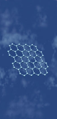
From buckyballs to graphine Buckyballs |
The problem is that the materials being used are reaching their fundamental limit. They become unstable when they are shaped into components that are smaller than ten nanometres in size (one nanometre being one-millionth of a millimetre). At this spatial scale, all current semiconductors, including silicon, will oxidise, decompose and migrate uncontrollably along surfaces, like water droplets on a hot plate.
Unlike all other known materials, however, graphene remains highly stable and conductive even when it is cut into devices one nanometre wide, while graphene transistors start showing advantages and good performance at sizes below ten nanometres – the miniaturisation limit at which silicon technology is predicted to fail.
‘It is too early to promise graphene supercomputers,’ says Professor Geim. ‘In our work, we rely on chance when making such small transistors. Unfortunately, no existing technology allows us to cut materials with true nanometre precision. But this is exactly the same challenge that all post-silicon electronics has to face. At least we now have a material that can meet such a challenge.’
Liquid crystal displays
But graphene also has more immediate applications. One of its other discoverers is Dr Kostya Novoselov, who is now also at Manchester, and, together with other colleagues, he has shown how you can use graphene as a transparent conductive coating for electro-optical devices like LCDs.
‘Its high transparency and low resistivity make it ideal for electrodes in liquid-crystal devices,’ explains Dr Novoselov. ‘These properties seem to make this material an excellent candidate for applications in various electro-optical devices that require films which are conducting, transparent and thin. We believe graphene should improve the durability and simplify the technology of potential electronic devices that interact with light.’
‘Transparent conducting films are an essential part of many gadgets, including common LCDs for computers, TVs and mobile phones,’ adds Professor Geim. ‘The underlying technology uses thin metal-oxide films based on indium. But indium is becoming an increasingly expensive commodity and its supply is expected to be exhausted within just ten years.
‘Forget about oil – our civilisation will run out of indium first. Scientists have an urgent task on their hands to find new types of conductive transparent films.’
The Manchester team has now demonstrated that highly transparent and highly conductive ultra-thin films can be produced cheaply by ‘dissolving’ chunks of graphite – an abundant natural resource – into graphene and then spraying the suspension onto a glass surface. The resulting graphene-based films can be used in LCDs, and, to prove the concept, the research team has created the first liquid-crystal devices with graphene electrodes.
Dr Novoselov believes that only a few small, incremental steps remain before this technology can reach a mass-production stage. ‘Graphene-based LCD products could appear in shops in just a few years,’ he says. ‘The fact is, though, that applications don’t only depend on the potential properties of the material; they also depend on the market context and how far industry is ready to embrace them. Silicon is not even the best material for transistors.
‘There are lots of semiconductors that are much better, but it is just not practical to move yet from the enormous capital investment in silicon to something else. In respect of our transistors, there is some interest from the giants, such as Intel and IBM, but it is hard to say when they will get into the factories.
‘The difference with our LCD displays is that it is not that costly to research new materials because the indium that is being used at the moment is already taking such a huge proportion of the cost.
‘I am confident, if we talk again in 20 to 30 years, that both applications will have been realised. If we speak again in five years, it will be LCDs that are in use anywhere you need a transparent conductive coating, such as in solar-cell or touch-screen technology.’
But, for the team in Manchester, graphene is more than just the sum of its potential applications. For Dr Novoselov, graphene is like a playground for physicists.
Fun for physicists
‘We are a small team here,’ he says, ‘and we do whatever is good fun. Graphene is a great playground because there are several fields of science involved, and you can test many theoretical models on it and so have a lot of fun. We really cover everything. Graphene is the first example of a material in which electrons mimic relativistic particles. Instead of having to go into accelerators or into space to study a phenomenon such as massless particles, you can see the effect and study them in graphene.
‘But the mechanical properties are amazing also. This is the strongest material in the world. It has bonds that are stronger than diamond. We can have great fun playing with the mechanical properties as we attempt to fold it, bend it, rip it or carve some features in it.’
Graphene dreams
‘Our dream is to be able to manipulate it precisely at the tiniest of scales,’ he adds. ‘We hope to be able to take it down to a few atoms in size. At the moment, we cut it a little, then check it and cut it again and, with this technique, we can create a piece of graphene a few atoms across. However, this technique is not well developed yet. We can do it in a lab, but it takes us several days to make a single structure and this is not acceptable for most situations in which you need to make one structure reliably in a few minutes.’
‘The real hurdle is that we do not actually have a technique to reliably make it small enough,’ agrees Professor Geim. ‘To create molecule-sized electronics, we need to take it controllably to the true nanometre scale. We can go to the 1,000-atom size very easily. If we try really hard, we can go to the 200-atom scale, but we need to get down to a scale in the order of 10 atoms. We don’t have the technique so far to do this, but the whole semiconductor industry is going in this direction.’
David Williams is a journalist and author specialising in graduate and postgraduate choices.
Read other Engineering research papers, including a 2006 research paper about Self-healing Spacecraft and 2007 research about Greener, Cleaner Energy For The Future.